Atom probe tomography (APT) exhibits unique advantages and capabilities such as atomic resolution (lateral resolution: 0.3-0.5 nm and depth resolution 0.1-0.3 nm), 3D information about the position of each atom in the analysed sample and chemical sensitivity down to atomic parts per million.
Principle of APT
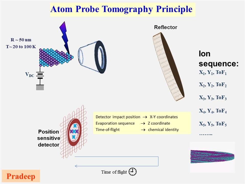
The prepared sample is cooled to ~ 50K in the analysis chamber. The tip is biased at high DC voltage (3-15 kV), generating a high electrostatic field sufficient to field evaporate atoms. By applying a voltage or laser pulse, evaporated ions are projected onto a position-sensitive detector. The Time of Flight (ToF) measurement allows for the reconstruction of the original atomic positions.
History and Evolution
In the 1950s, Erwin Wilhelm Müller developed the Field Ion Microscope (FIM). In 1969, Müller and Panitz added a Time-of-Flight mass spectrometer to detect specimen chemistry. Breakthroughs in the 1980s, including laser pulsing (Tsong & Kellogg) and position-sensitive detectors (Cerezo, Godfrey & Smith), transformed APT into the 3D atomic mapping tool used today.

Modern APT: LEAP 5000
The LEAP 5000 can extract 100,000 atoms per second, providing 3D atom-by-atom imaging at sub-nanometer resolution. NFAPT utilizes a CAMECA LEAP 5000 XR and an FEI Helios G4 dual beam system for high-precision research.
References
- CAMECA Atom Probe Instruments
- Atom Probe Tomography - Essential Knowledge briefings (John Wiley & Sons, 2017)